Indiana Microscopy Society
An Affiliate of the Microscopy
Society of America

|

|

|

|
 |

|
 |

|

|
|
|
Indiana Microscopy SocietyAn Affiliate of the Microscopy
|
|
Dear INMS Members,
The Indiana Microscopy Society 2014 Spring Meeting will be held April 17, 2014 at Purdue University following a Ted Pella Microwave Processing Work Shop, see Corporate News. More details later. Please mark your calendars today and plan to attend.
Your 2014 dues are due. If you joined at the Fall meeting you are paid for 2014. The dues are $10. Please note any changes to email address, print email clearly and neatly. You may use PayPal on the INMS web page or send a check payable to INMS to:
Mike Esterman, Secretary
Indiana Microscopy Society
7263 North Baltimore Rd
Monrovia, IN 46157
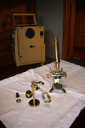
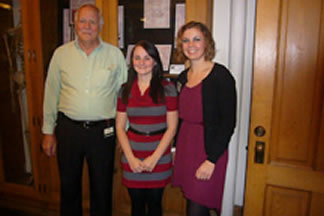
The attendees also had a guided tour of the museum with numerous vintage microscopes on display. The oldest was a brass scope built in 1857 by M. Pillscher, provided by Dr. Jim Smith. The tour was followed by a bountiful buffet before the meeting. The program was presented by Dr. George Sandusky, Ms Chelsea Dodge, and Ms Shannon Cook.
|
|
| 1857 Microscope | Speakers at the Fall meeting: George, Chelsea and Shannon |
Ted Pella
Microwave Workshop Sponsored by Ted Pella, Inc. - April 15-17 at Purdue University, Life Sciences Microscopy Facility
Course Topics: Tissue Processing for EM, Immunolabeling, and Fundamentals of Paraffin Tissue Processing Hands-On Techniques: Tissue Processing for EM, Immunolabeling.
Details and registration form are in the workshop attachment. Registration Deadline: April 1
The Indiana Microscopy Society Spring Meeting will follow the workshop on April 17.
Oxford Instruments
Please plan to visit Oxford Instruments in booth #3722 at PittCon 2014 this year (March 3-6,2014). We will have an SEM in our booth and we will be running live EDS demos with customer samples as well as demos of the new Large Area Mapping capability. Contact Nancy Crouch to schedule a time.
Bruker
If you would like to see a live demonstration of the Bruker EDS and/or EBSD at the March Pittsburgh Conference, please contact Mark Kelsey. If you are not attending, a live demonstration in your lab can be arranged as well.
Gatan
April 8-11, 2014 EELS School
On-line registration is now open at:
http://www.gatan.com/company/news/news11251302.php
or you can contact:
Steve Nagy - Gatan Inc., US Central Regional Business Mgr., Cell: (612) 616-9557
EELS mapping of large areas across wide energy windows. In a recent study, Gatan Analytical TEM investigators were able to acquire atomic level EELS elemental maps 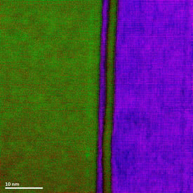 at 200 kV using a probe corrected TEM with cold-field emission gun (courtesy of IBM). The maps cover an area in the specimen of over 2500 nm2 and were obtained streaming over 1.1 million EELS spectra, at a spectral rate of 500 spectra per second. Each EELS spectrum covers an energy window from 250 eV to 2250 eV allowing every element in the specimen to be recorded and enabling defects to be studied at atomic resolution across interface regions.
Figure at right: EELS elemental maps of Ti L2,3 edges at 456 eV in green, Mn L2,3 edges at 640 eV in blue, La M4,5 edges at 832 eV in purple and Sr L2,3 edges at 1940 eV in red.
Gatan acknowledges Dr. Phil Rice and Dr. Teya Topuria of IBM in San Jose, CA for access to their microscope installation and providing both the TEM specimen and expert assistance in setting up the microscope.
Mager Scientific
From now until June 30, 2014, Mager Scientific is offering a free motorized stage with the purchase of a new Leica EM ACE Sputter Coater. Choose from low or high vacuum models and receive savings from $4,000 up to $10,000. For details and a short video demo, visit our website. Mager Scientific is your authorized dealer for Leica Microsystems EM Sample Preparation instruments.
Visit us at www.magersci.com or call 734.426.3885.
Jake Christensen, Mager Scientific, Inc.
734-426-3885
www.magersci.com
FEI
FEI is partnering with Materials Today to offer an exclusive webinar: Focused ion beam fabrication of resonant antennas for nanoscale imaging. Presented by Laurent Roussel, Product Marketing Manager SEM/DualBeam; and Rainer Hillenbrand, Ikerbasque Research Professor and Group Leader at CIC nanoGUNE.
Date/time: February 12, 2014: 4.00pm GMT, 5.00pm CET, 11.00am EST
Click here to join the webinar and learn more about using DualBeam FIB/SEM for rapid fabrication of 3D functional nanodevices.
Scott W. Shawmeker | Regional Account Manager FEI
6446 Fountains Blvd West Chester, Ohio 45069 USA
Tel 513 777 2347 Cell 513 885 0986
JEOL USA
If you are making preparations to attend Pittcon 2014 in Chicago next month, please join us for a press conference and hear the latest on mass spec and microscopy from JEOL. We look forward to seeing you!
Please join us for a lively afternoon presentation of new imaging and analytical technology from JEOL. We have two very knowledgeable and interesting speakers who will focus on two recent product introductions that are highlighted at Pittcon 2014.
Dr. Chip Cody, co-inventor of the DART (Direct Analysis in Real Time) ion source will describe recent developments in our mass spectrometry product line and collaborations with our partners. JEOL has explored new ways to make use of the high resolution, exact-mass data available from the AccuTOF GCV 4G time-of-flight mass spectrometer combined with comprehensive 2D gas chromatography. New sampling devices and software have improved the AccuTOF-DART’s throughput for quantitative and qualitative analysis. In addition, higher performance specifications for the SpiralTOF ultra-high performance MALDI TOF/TOF system are now available. Collaborations with our electron optics division have provided complementary data for several recent research products, highlighting the strengths of the different instrument types.
Vern Robertson, our SEM technical spokesman with decades of hands-on SEM experience covering a wide variety of applications, will discuss the fast microanalysis capabilities of the new iT300LV Scanning Electron Microscope. Smart analytical port geometries on the SEM allow for up to 11 analytical attachments and dual EDS (energy dispersive x-ray spectroscopy) and EBSD (electron backscatter diffraction) - - that makes it the most flexible, sleekest SEM around! Vern will also discuss how these two dramatically different techniques can be can be married together for "correlative microscopy" on a new level. The iT300LV is our latest InTouchScope research grade SEM and a great addition to any lab.
We will provide refreshments. Please stop by and join us for a half hour on this opening day of Pittcon!
Pamela Mansfield | Marketing Communications JEOL USA | 978.536.2309 | pmansfield@jeol.com www.jeolusa.com
| Applied Precision http://www.api.com/ |
Bruker http://www.bruker.at/ |
Carl Zeiss Microscopy http://www.zeiss.com/nts/ |
EDAX http://www.edax.com/ |
| Electron Microscopy Sciences http://www.emsdiasum.com/ |
FEI Company http://www.fei.com/ |
Gatan, Inc. http://www.gatan.com/ |
Hitachi HTA http://www.hitachi-hta.com/ |
| IXRF Systems, Inc http://www.ixrfsystems.com/ |
JEOL http://www.jeolusa.com/ |
Mager Scientific, Inc http://www.magersci.com/ |
Microscopy Innovations http://www.microscopyinnovations.com |
| Oxford Instruments www.oxford-instruments.com |
Ted Pella, Inc http://www.tedpella.com/ |
Mike Esterman, Secretary
Indiana Microscopy Society
7263 North Baltimore Rd
Monrovia, IN 46157
esterman@ccrtc.com